

As global demand for renewable energy continues to rise, photovoltaic (PV) manufacturers are under increasing pressure to improve production efficiency while maintaining long-term product reliability. Modern solar modules are expected to operate in outdoor environments for more than two decades, often under extreme temperature fluctuations, humidity, wind loads, and continuous ultraviolet exposure.
Achieving that level of durability begins during manufacturing.
One of the most critical challenges in solar production is identifying hidden defects inside silicon wafers and solar cells before they become costly failures in the field. Many of these defects are invisible under conventional lighting conditions and cannot be detected through manual inspection.
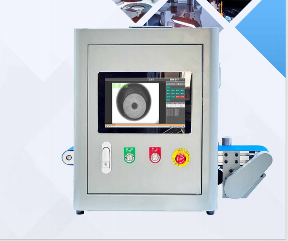
To address this challenge, manufacturers increasingly deploy automated inspection machines equipped with advanced imaging technologies such as Electroluminescence (EL), Photoluminescence (PL), and AI-driven defect analysis.
Why Micro-Crack Detection Matters in Solar Manufacturing
Silicon wafers are extremely thin and brittle.
Throughout production, wafers are exposed to multiple sources of mechanical and thermal stress, including:
- Wafer slicing
- Automated handling
- Cell stringing
- Soldering processes
- Module lamination
Even microscopic structural damage can gradually expand after installation.
Common consequences include:
- Reduced power generation
- Hot spot formation
- Accelerated module degradation
- Warranty claims
- Premature system failure
Because many of these defects cannot be observed with standard optical cameras, specialized inspection technologies are required.
Key Inspection Stages Across the PV Manufacturing Process
Wafer Inspection After Slicing
The production process begins with silicon ingots being sliced into ultra-thin wafers.
At this stage, inspection systems evaluate:
- Edge chipping
- Thickness consistency
- Surface scratches
- Micro-fissures
- Total Thickness Variation (TTV)
Removing damaged wafers before downstream processing helps reduce breakage and improves production yield.
Solar Cell Stringing Inspection
During cell interconnection, copper ribbons are soldered onto individual solar cells.
The localized heating process can introduce new defects, including:
- Thermal micro-cracks
- Ribbon misalignment
- Incomplete solder joints
- Cell damage caused by handling stress
Modern machine vision inspection systems monitor these processes in real time to prevent defective cells from entering module assembly.
Final Module Inspection
Before a solar panel is laminated and framed, manufacturers typically perform a comprehensive electrical and optical quality assessment.
This final inspection stage helps identify:
- Cracked cells
- Broken busbars
- Electrically inactive regions
- Cell mismatch issues
Detecting these defects before shipment significantly improves module reliability.
Understanding EL and PL Inspection Technologies
Traditional visible-light cameras can only inspect surface conditions.
Many critical PV defects exist inside the silicon crystal structure and require specialized inspection methods.
Photoluminescence (PL) Inspection
PL systems illuminate the wafer using a laser or controlled light source.
The silicon emits near-infrared radiation based on its crystalline condition.
By analyzing these emissions, manufacturers can detect:
- Internal cracks
- Crystal defects
- Material contamination
- Wafer stress regions
PL inspection is commonly used during early-stage wafer production.
Electroluminescence (EL) Inspection
EL testing applies electrical current to the solar cell.
Healthy regions emit infrared light, while damaged areas appear darker in the resulting image.
EL inspection is particularly effective for identifying:
- Micro-cracks
- Broken fingers
- Busbar interruptions
- Electrically inactive zones
Because EL directly reflects electrical performance, it remains one of the most widely adopted quality control methods in photovoltaic manufacturing.
High-Sensitivity Imaging with InGaAs Cameras
Capturing EL and PL images requires sensors capable of detecting weak infrared signals.
Standard CMOS and CCD cameras have limited sensitivity in these wavelengths.
For this reason, many advanced solar cell inspection systems utilize InGaAs (Indium Gallium Arsenide) sensors.
Key advantages include:
- High infrared sensitivity
- Faster image acquisition
- Improved defect contrast
- Reduced inspection cycle times
These capabilities support high-throughput production environments while maintaining inspection accuracy.
Artificial Intelligence in Solar Defect Classification
Modern solar production lines generate enormous quantities of inspection data.
Manual review of every EL image is impractical.
As a result, manufacturers increasingly integrate AI-powered defect detection models into inspection workflows.
Deep learning algorithms can automatically classify:
- Micro-cracks
- Finger interruptions
- Cell fractures
- Edge defects
- Process-induced damage
Compared with traditional rule-based systems, AI models can better adapt to variations in cell design and manufacturing conditions.
This helps reduce false alarms while improving defect detection consistency.
Frequently Asked Questions
What Causes Hot Spots in Solar Panels?
Hot spots occur when damaged or defective cells create localized electrical resistance.
These areas generate excess heat during operation, reducing module efficiency and potentially shortening service life.
Early EL inspection helps identify the defects that commonly lead to hot spots.
What Is the Difference Between EL and PL Inspection?
PL inspection evaluates material quality before electrical contacts are fully formed.
EL inspection evaluates electrical behavior after cell processing.
Both technologies provide valuable information and are often used together in advanced PV manufacturing facilities.
Can AI Distinguish Between Surface Scratches and Structural Cracks?
Yes.
Modern deep learning models analyze geometric patterns, defect morphology, and electrical signatures to differentiate cosmetic surface marks from structural defects that may affect long-term performance.
Conclusion
As photovoltaic manufacturing continues to scale globally, quality control remains a critical factor in achieving reliable module performance and reducing long-term warranty risks.
By implementing automated inspection machines, machine vision inspection systems, Electroluminescence testing, Photoluminescence analysis, and advanced AI-powered defect detection, manufacturers can identify hidden defects before they reach the field.
These technologies not only improve production yield but also help ensure that solar modules deliver stable energy output throughout their expected service life.
Leave a Reply